The Foundation of Every Optical System Starts with a Single Lens
No matter how sophisticated your optical design may be, its real-world performance ultimately depends on the physical precision of each lens element. A theoretical spot size of half a micron means nothing if surface form error, subsurface damage, or inconsistent centering pushes the actual beam waist beyond tolerance.
At Eata Ray, we provide end-to-end lens processing services built exclusively for the research community. Our fabrication pipeline covers everything from raw blank preparation through final metrology, giving academic labs, government research institutes, and technology startups a dependable path from optical prescription to physical component.
Whether your project calls for a single prototype achromat or a small batch of aspheric condensers, our team works directly with your specifications without imposing rigid minimum order quantities.
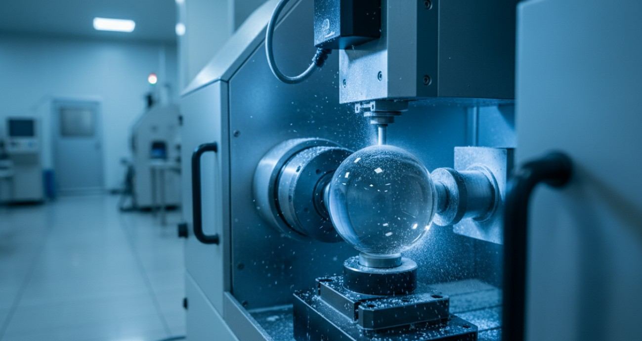 Figure 1. CNC precision grinding of an optical lens blank on a 5-axis machining center.
Capabilities Across the Full Fabrication Chain
Precision lens manufacturing is not a single operation. It is a sequential chain of controlled material removal steps, each of which must be carefully matched to the substrate material, surface geometry, and target figure accuracy. Our facility maintains in-house capability across every critical stage.
CNC Grinding and Precision Shaping
The journey from optical blank to finished lens begins with deterministic grinding. Using 5-axis CNC optical grinding centers, we shape spherical, aspherical, and plano surfaces with sub-micron control over sagitta and center thickness.
- Rough grinding with diamond cup tools removes bulk material and establishes the nominal radius of curvature.
- Fine grinding with sequentially finer abrasive grits reduces subsurface damage while converging toward the target dimensional tolerance.
- In-process probing verifies sagitta and thickness before the optic ever leaves the grinding station, catching deviations early when they are still inexpensive to correct.
Deterministic Polishing Technologies
After grinding, the surface must be smoothed to eliminate fracture damage and bring the form into specification. We deploy multiple polishing modalities, selecting the most appropriate based on geometry complexity, material hardness, and figure tolerance.
- Computer-controlled polishing (CCP) uses a small tool driven by surface error maps from interferometry, selectively removing material only where needed.
- Magnetorheological finishing (MRF) offers deterministic correction for aspheres and freeforms, achieving figure accuracy below 0.1 wave PV and surface roughness under 5 angstroms RMS.
- Traditional pitch polishing remains our go-to method for super-polishing applications where atomic-level smoothness is required, such as high-power laser optics or EUV mirror substrates.
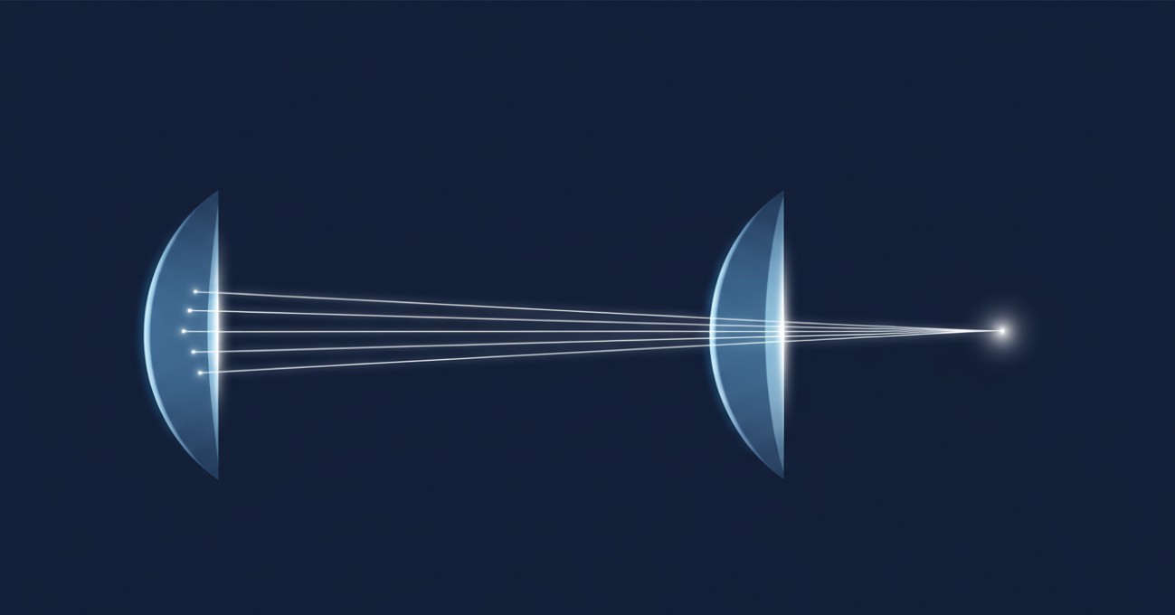 Figure 2. Cross-sectional comparison showing how an aspherical lens eliminates spherical aberration for tighter focal spot convergence.
Aspherical and Freeform Surface Expertise
Rotation-symmetric aspheres and fully freeform surfaces present unique manufacturing challenges because the local curvature varies continuously across the aperture. Conventional spherical tooling cannot adapt to these variations, which is why deterministic sub-aperture methods are essential.
Our aspheric workflow combines stylus profilometry for mid-spatial-frequency characterization with stitching interferometry for full-aperture form verification. For freeform surfaces, we accept design definitions in multiple formats, including Zernike polynomial coefficients, XY point clouds, and NURBS surfaces.
Achievable specifications include form error down to 0.5 micrometer PV on infrared aspheres, surface roughness below 1 nanometer RMS on fused silica, and departure from best-fit sphere up to 20 millimeters depending on part diameter.
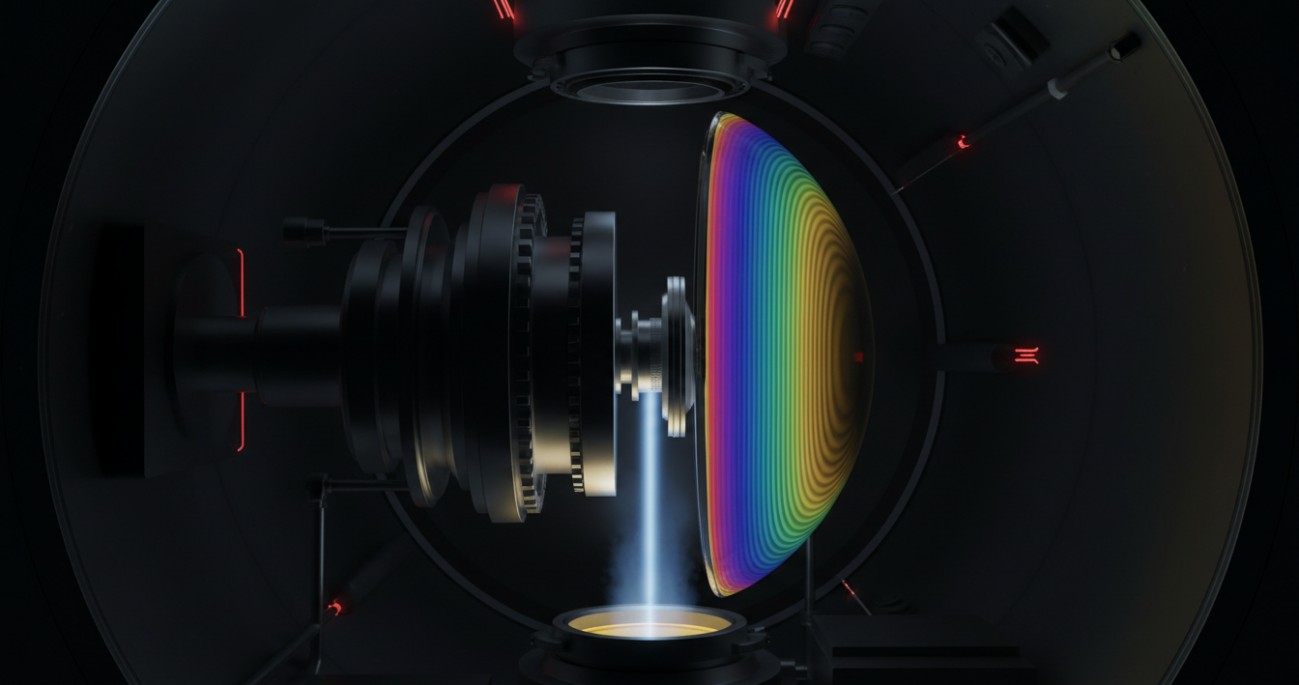 Figure 3. Electron-beam deposition of multilayer dielectric coating inside a high-vacuum chamber.
Thin-Film Coating Deposition
An uncoated lens reflects roughly 4 percent of incident light at each surface. In a multi-element assembly, those losses compound rapidly, degrading throughput and introducing ghost images. Our in-house coating capability addresses this with tailored thin-film solutions.
We offer anti-reflection coatings from the ultraviolet through the long-wave infrared, optimized for specific center wavelengths or broadband performance. High-reflectivity dielectric stacks, beamsplitter coatings, and narrowband filters are also available.
Deposition technologies include ion-assisted electron-beam evaporation for dense, environmentally stable films, and ion beam sputtering for applications demanding the lowest absorption and highest laser damage thresholds.
Materials and Achievable Specifications
Our grinding and polishing systems accommodate a broad spectrum of optical materials, from conventional glasses to advanced ceramics and infrared crystals. The table below summarizes the typical parameter ranges we hold across our standard fabrication workflows.
| Parameter |
Range / Options |
Notes |
| Part Diameter |
3 mm to 300 mm |
Larger parts upon review |
| Center Thickness |
Down to 0.5 mm |
Ultra-thin down to 100 µm for special substrates |
| Radius of Curvature |
2.5 mm to infinity (plano) |
Concave and convex, limited by tooling |
| Surface Figure (Spherical) |
λ/10 to λ/4 @ 632.8 nm |
λ/10 achieved via MRF finishing |
| Surface Roughness |
< 0.5 nm RMS (super polish) |
Typical 1-3 nm RMS for standard polish |
| Surface Quality |
10-5 scratch-dig |
Per MIL-PRF-13830B |
| Centering Tolerance |
< 1 arcmin beam deviation |
Precision centering with air-bearing spindles |
| Edge Treatments |
Bevels, protective chamfers, edge blackening |
RoHS-compliant ink for stray-light suppression |
| Coating Wavelength |
193 nm to 15 µm |
AR, HR, beamsplitter, filter designs |
Research Applications We Support
Our lens processing services have supported a diverse portfolio of research programs. Representative application areas include:
- High-power laser systems: Large-aperture fused silica lenses with super-polished surfaces and high-damage-threshold AR coatings for fusion energy research and materials processing.
- Microscopy and bioimaging: Custom objective components including plano-convex and meniscus condensers with tight centering tolerances for light-sheet and confocal instruments.
- Astronomical instrumentation: Off-axis aspheric mirrors and corrector plates with low mid-spatial-frequency error for adaptive optics and wide-field survey telescopes.
- Spectroscopy: Precision cylindrical lenses and toroidal elements for Rowland-circle spectrometers and optical parametric oscillator pump beams.
- Quantum optics: Ultra-low-loss windows and lenses with sub-nanometer roughness for cavity quantum electrodynamics experiments and squeezed light sources.
- Infrared thermal imaging: Ge, ZnSe, and chalcogenide glass aspheres with broadband AR coatings for SWIR, MWIR, and LWIR detection systems.
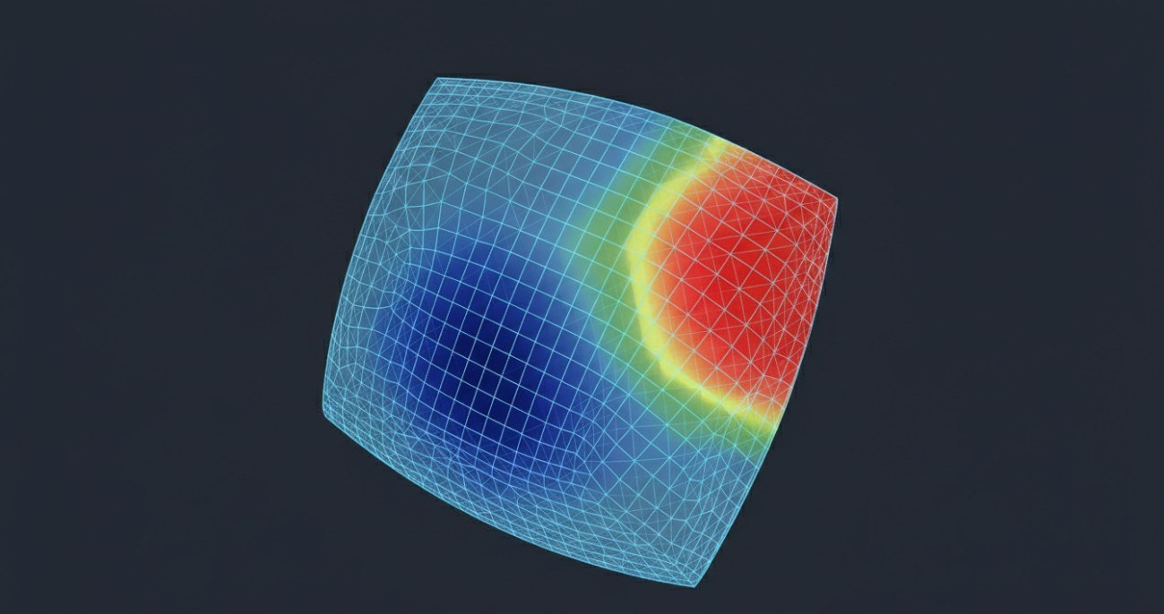 Figure 4. Surface topology map of a freeform optical element showing nanometer-level sag deviation across the aperture.
Quality Verification and Metrology
Fabrication without measurement is guesswork. Every lens that leaves our facility has passed through a structured metrology protocol appropriate to its specification level.
Our metrology lab is equipped with phase-shifting interferometers for surface figure verification, white-light profilometers for roughness characterization, and coordinate measuring machines for dimensional and geometric tolerance confirmation.
For aspheres and freeforms, we deploy sub-aperture stitching interferometry to reconstruct full-aperture surface data from overlapping partial measurements. Computer-generated holograms (CGHs) extend this capability to conic and polynomial aspheres where conventional null lenses would be impractical.
Each shipment includes a detailed inspection report documenting measured surface figure, center thickness, wedge angle, surface roughness, and coating spectral performance where applicable.
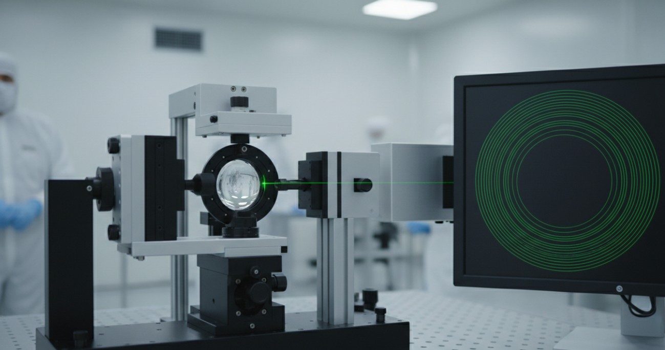 Figure 5. Sub-aperture stitching interferometry in our metrology lab verifying surface figure of a precision lens.
How to Engage Our Lens Processing Service
We have structured our workflow to accommodate the unpredictable timelines and evolving requirements that are inherent to research. There are no rigid procurement portals or locked-in specifications. Changes mid-process are handled transparently with revised delivery estimates.
- Requirement Review: Send us your lens drawing, optical prescription, or even a conceptual description. Our engineers assess material selection, manufacturability, and the appropriate fabrication route.
- Technical Proposal: Within 48 hours, you receive a detailed quotation including achievable tolerances, surface specification, coating recommendation, estimated lead time, and unit pricing.
- Prototype Fabrication: For first-time designs, we typically produce one to three prototype units. This allows optical performance validation in your system before committing to a larger batch.
- Measurement and Reporting: Every part is fully characterized in our metrology lab. You receive raw measurement data alongside a summary inspection report.
- Delivery and Follow-Up: Lenses are carefully packaged and shipped with full traceability documentation. Our engineers remain available for integration support and design iteration discussions.
Request a Technical Consultation
If you have a lens design that needs to move from concept to reality, we are ready to review your requirements. There is no charge for initial feasibility assessment, and we welcome unconventional geometries that push the boundaries of conventional optical manufacturing.
Get in touch today and receive a detailed processing proposal tailored to your research timeline and performance targets.


